
|
||||||
|
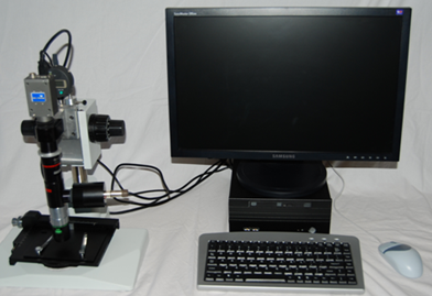
Overview
|
||
Applications
|
|||
Standard Features |
Optional Features |
||
ICS1000NIR Image Gallery |
|||
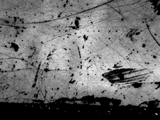
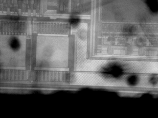
IC Backside NanoPrep <<IC Surface IC Circuitry>>
Inspection of the work surface of a flip-chip IC during backside prep is important to ensure quality results. The image to the left is the surface of a device being backside prepped using the state-of-the-art RKD NanoPrep. The device is being readied for backside photon emission. No attempt was made to remove all the debris on the surface for this image capture. The ICS1000NIR was then focused down to the circuitry below. This is the image to the right. The remaining silicon thickness measured with the ICS1000NIR in this example is 220um. Note how the integrated monochromatic illuminator of our system can penetrate the backside silicon and generate sharp images, even with the debris! |
|||
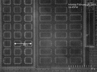
IC Backside Imaging through 53um of silicon. 140X optical mag; ICS1000 Imaging Software Suite can automatically label image with date, time, and scale information at the press of a button. |
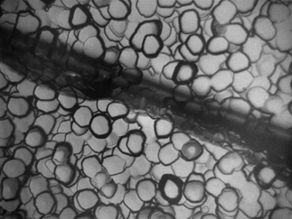
View of monocrystalline silicon solar cell with a microcrack; 20x objective |
||
2994 Scott Boulevard | Santa Clara, CA 95054 | Voice:(408)235-8690 | eFAX:(888)625-4418 | email: info@reltron.com |
|||
© 2009 Reltron LLC. All rights reserved. |
|||